Contents
Overview
Materials science tools are the sophisticated instruments that enable scientists and engineers to probe, characterize, and manipulate matter at scales ranging from the atomic to the macroscopic. These tools are fundamental to understanding the intricate relationship between a material's structure, its properties, and its ultimate performance. From electron microscopes revealing atomic lattices to spectrometers analyzing elemental composition, these technologies drive innovation across diverse fields like aerospace, medicine, and electronics. The development and application of these tools have historically been intertwined with major technological advancements, such as the transistor and advanced alloys, and continue to push the boundaries of what is possible in material design and discovery. Without these instruments, the very concept of designing materials for specific functions would remain largely theoretical, confined to empirical trial-and-error rather than precise, predictive engineering.
🎵 Origins & History
The lineage of materials science tools stretches back to the earliest attempts to understand metals and minerals. Early metallurgists in ancient civilizations relied on rudimentary tools like furnaces and hammers, observing how heat and force altered materials. The Enlightenment era saw the application of more scientific methods, with early spectroscopes and microscopes beginning to reveal elemental compositions and microstructures. The 20th century marked a revolution, driven by the need for advanced materials during wartime and the subsequent boom in electronics. The invention of the transmission electron microscope (TEM) provided unprecedented views of atomic arrangements, while X-ray diffraction techniques became indispensable for determining crystal structures. The development of scanning electron microscopy (SEM) further democratized high-resolution imaging, making these powerful analytical capabilities more accessible.
⚙️ How It Works
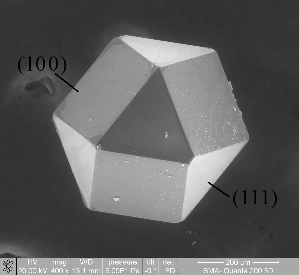
Materials science tools operate on diverse physical principles to interrogate matter. Microscopy techniques, such as Scanning Probe Microscopy (SPM) (including Atomic Force Microscopy (AFM) and Scanning Tunneling Microscopy (STM)), use sharp probes to scan surfaces, mapping topography and local electronic properties with atomic precision. Electron microscopy (TEM and SEM) employs beams of electrons, which have much shorter wavelengths than visible light, to achieve resolutions far beyond optical microscopes, revealing internal structures and surface morphologies. Spectroscopic methods, like X-ray Photoelectron Spectroscopy (XPS) and Energy-dispersive X-ray Spectroscopy (EDS), analyze the characteristic X-rays or electrons emitted or absorbed by a material when bombarded with high-energy particles, thereby identifying elemental and chemical composition. Diffraction techniques, such as X-ray Diffraction (XRD), use the scattering patterns of X-rays or neutrons to determine crystal structure and phase identification.
📊 Key Facts & Numbers
The global market for materials characterization equipment is substantial, with estimates placing it in the tens of billions of dollars annually. For instance, the electron microscopy market alone was valued at over $5 billion in 2023, with projections indicating continued growth. AFM systems can achieve vertical resolutions of less than 0.1 nanometers, enabling the visualization of individual atoms. XRD instruments can analyze samples in minutes, providing detailed crystallographic information. The cost of advanced materials science tools can range from tens of thousands of dollars for basic optical microscopes to over $1 million for high-end TEM systems. A single SEM might analyze hundreds of samples per day in a busy industrial lab, generating terabytes of imaging data annually. The precision of these tools is paramount; for example, measuring lattice strain with Digital Image Correlation (DIC) can achieve sub-micron accuracy.
👥 Key People & Organizations
Key figures in the development of materials science tools include Ernst Ruska, co-inventor of the electron microscope, and Richard Feynman, whose 1959 lecture 'There's Plenty of Room at the Bottom' inspired nanotechnology and the development of tools to manipulate matter at the atomic scale. Major manufacturers of these sophisticated instruments include Thermo Fisher Scientific, Carl Zeiss AG, JEOL Ltd., and Bruker Corporation. Research institutions like MIT, Stanford University, and the Max Planck Society are at the forefront of developing novel characterization techniques and pushing the capabilities of existing tools. Organizations such as the Materials Research Society (MRS) play a crucial role in disseminating research and fostering collaboration among users and developers of these tools.
🌍 Cultural Impact & Influence
Materials science tools have profoundly shaped modern technology and our understanding of the physical world. The ability to visualize and analyze materials at the nanoscale was critical for the development of the integrated circuit and the subsequent digital revolution. Advances in alloy development for aerospace and automotive industries, enabled by precise characterization, have led to lighter, stronger, and more fuel-efficient vehicles. In medicine, tools like X-ray crystallography have been instrumental in determining the structures of proteins and drug molecules, paving the way for targeted therapies. The visual output from electron microscopes, often stunning in their complexity, has also captured public imagination, bridging the gap between abstract science and tangible reality, and influencing art and design.
⚡ Current State & Latest Developments
The current landscape of materials science tools is characterized by increasing integration of artificial intelligence and machine learning for data analysis and instrument control. Automation is a major trend, with robotic sample handling and automated data acquisition becoming standard in high-throughput research environments. In-situ characterization, where materials are analyzed while undergoing testing (e.g., under stress, heat, or in a chemical environment), is gaining prominence, offering dynamic insights into material behavior. The development of correlative microscopy, which combines data from multiple techniques (e.g., AFM and SEM) on the same sample, provides a more comprehensive understanding. Furthermore, there's a growing demand for portable and field-deployable analytical tools, moving characterization beyond the lab. Companies like Oxford Instruments are developing advanced portable EDS systems for on-site analysis.
🤔 Controversies & Debates
One ongoing debate centers on the accessibility and cost of cutting-edge materials science tools. While powerful instruments are becoming more capable, their high price tags can limit their availability to well-funded institutions and corporations, potentially creating a divide in research capabilities. Another point of contention is the interpretation of complex data generated by these tools; while AI can assist, the expertise required for accurate analysis and avoiding misinterpretation remains a critical bottleneck. There's also a discussion about the environmental impact of manufacturing and operating these energy-intensive instruments, prompting research into more sustainable designs and operational practices. The proprietary nature of some advanced software used with these tools also raises concerns about data sharing and reproducibility within the scientific community.
🔮 Future Outlook & Predictions
The future of materials science tools points towards even greater integration with computational methods and AI. Expect instruments that can not only characterize but also predict material behavior with higher accuracy, potentially leading to 'self-optimizing' materials design workflows. The development of 'lab-on-a-chip' devices integrating multiple analytical functions into compact, portable systems will likely accelerate. Quantum sensing technologies may offer new avenues for ultra-sensitive measurements of magnetic, electric, and mechanical properties. Furthermore, tools capable of in-operando characterization of materials within complex devices, such as batteries or catalysts during operation, will become increasingly sophisticated, providing real-time feedback for performance optimization and failure analysis. The push for higher spatial and temporal resolution will continue, enabling the study of dynamic processes at the atomic scale.
💡 Practical Applications
Materials science tools are indispensable across a vast array of industries. In semiconductor manufacturing, tools like [[
Key Facts
- Category
- technology
- Type
- topic